




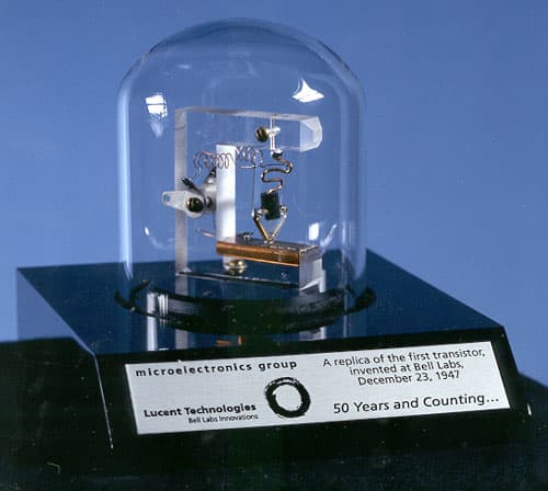
Every conversation you have with an AI model, every frame a graphics card renders, every phone in every pocket — all of it runs on physical objects that somebody had to manufacture. The blog has already told the story of the company that designs the chips AI runs on and the story of the lab that trains the models. This is the story of the layer underneath both: the company that actually makes the silicon.
TSMC does not design a single chip it sells. That is the entire point, and it was the strangest business idea in the semiconductor industry in 1987. This is how a man who failed his doctorate, chose a job over one dollar, and spent twenty-five years obsessed with a single manufacturing statistic ended up building the most consequential factory network on earth. 🧬
TL;DR: TSMC was founded in February 1987 on a promise no chip company had made: we will build your chips and never design our own. That guarantee created the fabless industry. TSMC is now worth roughly $2.16 trillion (23 July 2026) and makes about 90% of the world's leading-edge logic. See what AI builds on top of it →
🏭 What Is TSMC?
Taiwan Semiconductor Manufacturing Company was incorporated on 21 February 1987 in Hsinchu, Taiwan, as the world's first pure-play foundry — a chip factory whose only business is manufacturing other companies' designs. By most estimates it now produces roughly 90% of the world's leading-edge logic (5nm and below) and about 70% of the total foundry market including mature nodes.
| Metric | Value (as of 23 July 2026) |
|---|---|
| Founded | 21 February 1987, Hsinchu, Taiwan |
| Founder | Morris Chang (張忠謀), aged 55 at founding |
| Business model | Pure-play foundry — manufactures only, designs nothing |
| Market capitalization | ~$2.16 trillion — 6th most valuable company in the world |
| Leading-edge logic share | ~90% at 5nm and below (by most estimates) |
| Total foundry market share | ~70% including mature nodes |
| US expansion | Six-fab complex in Arizona; $6.6B CHIPS Act support against a $165B+ company commitment |
Two of those numbers deserve care. The market cap is a dated figure — TSMC crossed $2 trillion on 25 February 2026 and rose roughly 93% over the preceding twelve months, so any TSMC valuation quoted without a date is probably already wrong. And the 90% figure applies specifically to leading-edge logic; the car in your driveway is full of mature-node silicon from dozens of other fabs.
What makes TSMC unusual is not scale. It is the shape of the business. Before 1987, if you wanted to sell a chip, you had to own a factory. TSMC broke that requirement and brought an entire industry into existence.
🔀 What Is a Pure-Play Foundry, and Why Didn't It Exist Before 1987?
A pure-play foundry manufactures designs owned by other companies and owns none of its own. Integrated device manufacturers — Intel, Texas Instruments, NEC — had sold spare capacity for years, but they also sold competing chips, so handing over a design meant arming a rival. TSMC's innovation was contractual, not technical: it promised never to compete with its customers.
Read that diagram left to right and you are looking at the most consequential interface in modern computing. On the left, a designer with an idea and no factory. On the right, a factory with no ideas of its own. The arrow between them is worth trillions of dollars, and it did not exist until a 55-year-old executive who had just been passed over for promotion drew it.
One precision point: TSMC did not invent the foundry. It invented the pure-play foundry — and Chang had already pitched the idea inside Texas Instruments in 1976 and been turned down. He carried a rejected proposal for eleven years before he found a company to build it with.
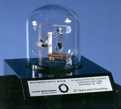
The idea is older than that pitch, though, and Chang said so himself in 2007. His very first assignment at Texas Instruments, in 1958, was running a production line manufacturing a transistor that IBM had designed and prototyped but did not want to build at volume:
"That was really very simply foundry work… and I also knew what the key was to successful custom work — that is, satisfying the customer."
So the pure-play foundry was not a flash of insight in 1985, or even a rejected memo in 1976. It was a thirty-year-old professional habit that finally got a company built around it. That is the more useful version of the story: the idea was never the scarce thing.
🌏 Who Is Morris Chang?
Morris Chang was born on 10 July 1931 in Ningbo, Zhejiang — not Taiwan, a place he would not visit until 1968 and not live in until 1985. By the age of eighteen he had fled war three times, lived in six cities, and changed schools ten times. That accounting is his own, not a biographer's.
The sequence reads like a map of a collapsing century. Guangzhou, where his father was a bank manager. British Hong Kong, after Japan bombed the city in 1937. Japanese-occupied Shanghai. Then, in late March 1943, a fifty-day crossing of the front lines into "Free China," ending at Chongqing and a place at the selective Nankai Middle School.
He wanted to be a writer. His father's verdict, as Chang reproduces it in his memoir: 「會餓肚子的」— "You'll go hungry."
In July 1949, days after his eighteenth birthday, he flew Pan Am out of Hong Kong's Kai Tak airport to San Francisco. He wrote in his diary aboard the plane: "Lifting into the sky, I looked back with a heavy heart; Hong Kong was already lost in the clouds… crossing an ocean to a country I did not know, the road ahead utterly obscure — how could I not feel sorrow?"
One year at Harvard — the only Chinese student in his class — then a transfer to MIT for mechanical engineering (BS 1952, MS 1953). His stated reason for transferring was job prospects.
Then the door closed.
🚪 Why Did Morris Chang Call Failing His Doctorate "The Greatest Stroke of Luck in My Life"?
Chang failed the MIT doctoral qualifying exam twice. He described the moment as "the greatest blow of my life. My self-esteem and self-confidence were destroyed in an instant." Decades later, having built TSMC, he called the same failure "the greatest stroke of luck in my life" — because a doctorate would have routed him into academia and away from semiconductors entirely.
It is worth being careful with that second quote. It is a founder narrating an accident in hindsight, which is a genre with a known bias. What it does establish is the shape of the life: the closed door pushed him into industry, and industry pushed him into a factory, and the factory is where he found the idea he would spend forty years on.
The rejection had one immediate consequence. Instead of a doctorate, he needed a job.
💵 How Did One Dollar Send Morris Chang Into Semiconductors?
Chang had four job offers and was leaning toward Ford — stable, prestigious, the safe choice. Ford offered $479 a month. Sylvania offered $480. He phoned Ford to ask about the difference and was told:
"We do not haggle. The company has decided on your salary. If you want to join, come. If not, then farewell."
He chose Sylvania over one dollar and a tone of voice. That decision put a mechanical engineer inside a brand-new transistor lab, where he had to teach himself device physics from William Shockley's 1950 textbook, Electrons and Holes in Semiconductors. His method was unglamorous and effective: he brought the book to the bar after work and bought drinks for senior colleagues so they would answer his questions about it.
He also carried one sentence out of Sylvania, from the semiconductor division's general manager, that he says he organized a career around:
"Our trouble at Sylvania is that we cannot make what we can sell and we cannot sell what we can make."
Sylvania was betting on germanium. A small company in Dallas was mass-producing silicon. In 1958, Chang joined it.
📉 What Is Yield, and Why Is It the Master Metric of Chipmaking?
Yield is the share of dies on a wafer that come out working. It is driven by defect density and falls exponentially as die size grows, because a bigger die is a bigger target for the same random contamination. Yield is the number the whole business turns on: a wafer costs the same to process whether its dies pass or fail, so raising yield collapses cost per good chip without adding a single machine.
Texas Instruments handed the 24-year-veteran-to-be that exact problem on his arrival in 1958. He took a near-zero line to roughly 20–30%, and built a reputation as someone who understood manufacturing at the level of physics rather than management. TI thought highly enough of him to pay full salary and tuition to send him to Stanford; he came back two and a half years later with a PhD in electrical engineering (1964).
The arithmetic he was fighting is unforgiving. The simplest textbook model treats defects as randomly scattered across the wafer, which gives yield as Y = e^(-D₀ × A) — where D₀ is defects per square centimetre and A is die area:
| Die area | Yield at D₀ = 0.1 /cm² | What this means |
|---|---|---|
| 10 mm² (small controller) | ~99% | Almost everything works |
| 50 mm² | ~95% | Still comfortable |
| 100 mm² (1 cm²) | ~90% | Every tenth die is scrap |
| 400 mm² | ~67% | A third of the wafer is thrown away |
| 800 mm² (large AI die) | ~45% | More than half the wafer is scrap |
Those are illustrative numbers from a standard model, not TSMC's internal figures — but the shape is real, and it is why the biggest chips in the world are the hardest ones to make money on. Double the die and you do not lose twice as much. You lose exponentially more.
(Every term in this section — yield, defect density, die, wafer, binning, tapeout — is defined in our AI compute and semiconductor glossary, along with the GPU and CUDA vocabulary that follows later.)
🇯🇵 What Did the 1981 Miho Discovery Reveal?
In 1981, Texas Instruments found that its Miho fab in Japan was running memory yields of 40–50% — roughly double the yields at its Houston fab. Chang was sent to find out why. What he found was not a machine. It was ~2% employee turnover in Japan against 10–25% in Houston, and technically educated shift leaders and equipment engineers standing on the line.
In the Japanese fab, the people who knew how the equipment behaved on a bad night were still there the following year, and the year after that. In Houston they were not, because top American engineering graduates would not take factory-floor jobs at all. (Chang's own retelling adds that the leading candidate for one US supervisor slot held a degree in French literature; that detail comes from him and is not independently verified.)
Yield, it turned out, was not primarily a physics problem. It was an institutional memory problem. The conclusion Chang drew was blunt: the future of advanced manufacturing was not in the United States. Six years later, he would act on it.
🚶 Why Did Morris Chang Leave Texas Instruments at 51?
By the late 1970s, Texas Instruments was pivoting toward calculators and digital watches, and the man who had spent his career on manufacturing physics was watching the company move away from him. After 25 years, at 51, with no realistic path to chief executive, Chang resigned with nothing lined up.
He became president and chief operating officer of General Instrument in New York. The work was acquisitions, and it bored him.
What mattered in that stretch was a single conversation. Gordon Campbell — later a co-founder of Chips and Technologies, one of the first fabless semiconductor companies — approached Chang while trying to raise $50 million for a chip company. Campbell came back some time later and said he now needed only a fraction of that, because he had subcontracted the fabrication instead of building a fab.
That was the proof. Design and manufacturing had quietly become two different businesses, and only one of them required a billion-dollar plant. Chang had proposed exactly this arrangement at TI in 1976 and been refused. Now somebody had done it accidentally, and the numbers worked.
🏗️ How Did TSMC Actually Get Founded in 1987?
K.T. Li — conventionally called the godfather of Taiwan's technology industry — recruited Chang to head ITRI in 1985 and told him the government wanted Taiwan to have a semiconductor company. It was effectively a blank cheque with no product attached. The pure-play foundry was Chang's answer to that brief, devised afterwards — not a plan he was hired to execute.
In February 1987 TSMC was incorporated on a promise no chip company had ever made:
We will build your chips, and we will never design our own.
The bet was contractual rather than technical. A fabless startup could hand over its crown-jewel design without arming a competitor, because the factory had no products of its own to defend. That single guarantee of neutrality is what made the fabless industry possible: thousands of designers who could never have afforded a fab, and one foundry whose scale came from serving all of them at once.
It did not look inevitable. Intel refused to invest. Then in late 1987, roughly nine months after incorporation, Andy Grove turned up to inspect the fab. Intel ran TSMC through its qualification process. TSMC passed, and Intel became its first American customer, ordering legacy 1.5-micron parts.
It is worth killing a myth here. The story is often told as Chang setting out to take on the giants of the day. He did not. The foil was never a company — it was the integrated model itself, the arrangement in which one firm both designs and manufactures. Intel became a customer, not a target. And the Korean chip industry that would eventually enter foundry work was not a factor in 1987 at all; that competition arrives roughly thirty years later.
✉️ How Did TSMC and NVIDIA Find Each Other?
In 1997, NVIDIA was down to about 60 people and nearly out of money. Jensen Huang had got nowhere with TSMC's San Jose sales office, so he mailed a letter. It reached Morris Chang, who telephoned him unannounced. The deal was signed in 1998, and it has compounded for nearly thirty years.
There is a second version of this story, and it has better sourcing. In October 2007, at the Computer History Museum, Huang interviewed Chang on stage — and told it with Chang sitting beside him, able to correct him. In that telling there is no letter. NVIDIA was founded in 1993, Huang called TSMC's local sales office, and nobody called him back:
"Let it go on record that I tried to call Morris. I just didn't get a call back."
By 1996 the relationship had changed, and by 1997 the two men were meeting. Both accounts may describe different moments of the same courtship — but when one version has the other participant in the room, prefer it, and don't merge them into a single tidy anecdote.
And the chip itself is more complicated than it is usually told. The original RIVA 128 (NV3) shipped on 25 August 1997 built by SGS-Thomson on a 350nm process in Crolles, France — NVIDIA's fab partner since NV1. The primary source settles it in NVIDIA's own words. NVIDIA's S-1 registration statement, filed 6 March 1998, states that the RIVA 128 graphics processor was "currently fabricated for the Company by ST".
But that is only the original part. NVIDIA subsequently moved the RIVA 128 ZX to TSMC, so the NV3 generation was manufactured by both companies, and the RIVA TNT (NV4, 31 August 1998) was the first fully-TSMC NVIDIA part.
So the flat claim "TSMC made the RIVA 128" is wrong, and so is the flat denial — which is itself a small lesson in the subject of this article. NVIDIA did not change foundries out of loyalty or romance. It changed because of yield.
(One honest caveat: whether ST was dropped outright on the ZX or retained as a second source is genuinely contested across the enthusiast record. The part that is not contested is the S-1 line above.)
For Chang's 2018 retirement, Huang commissioned an artist-rendered comic timeline of their friendship, which hangs in Chang's Taipei office. In the accompanying letter, read at the retirement dinner, Huang wrote that Chang's career was "a masterpiece, like Beethoven's Ninth Symphony."
🎯 What Happened When NVIDIA Optimized for Cost Instead of Developers?
It nearly died. The story is worth telling here because it is the customer's side of the same manufacturing economics — and because Huang's verdict on it is four words long.
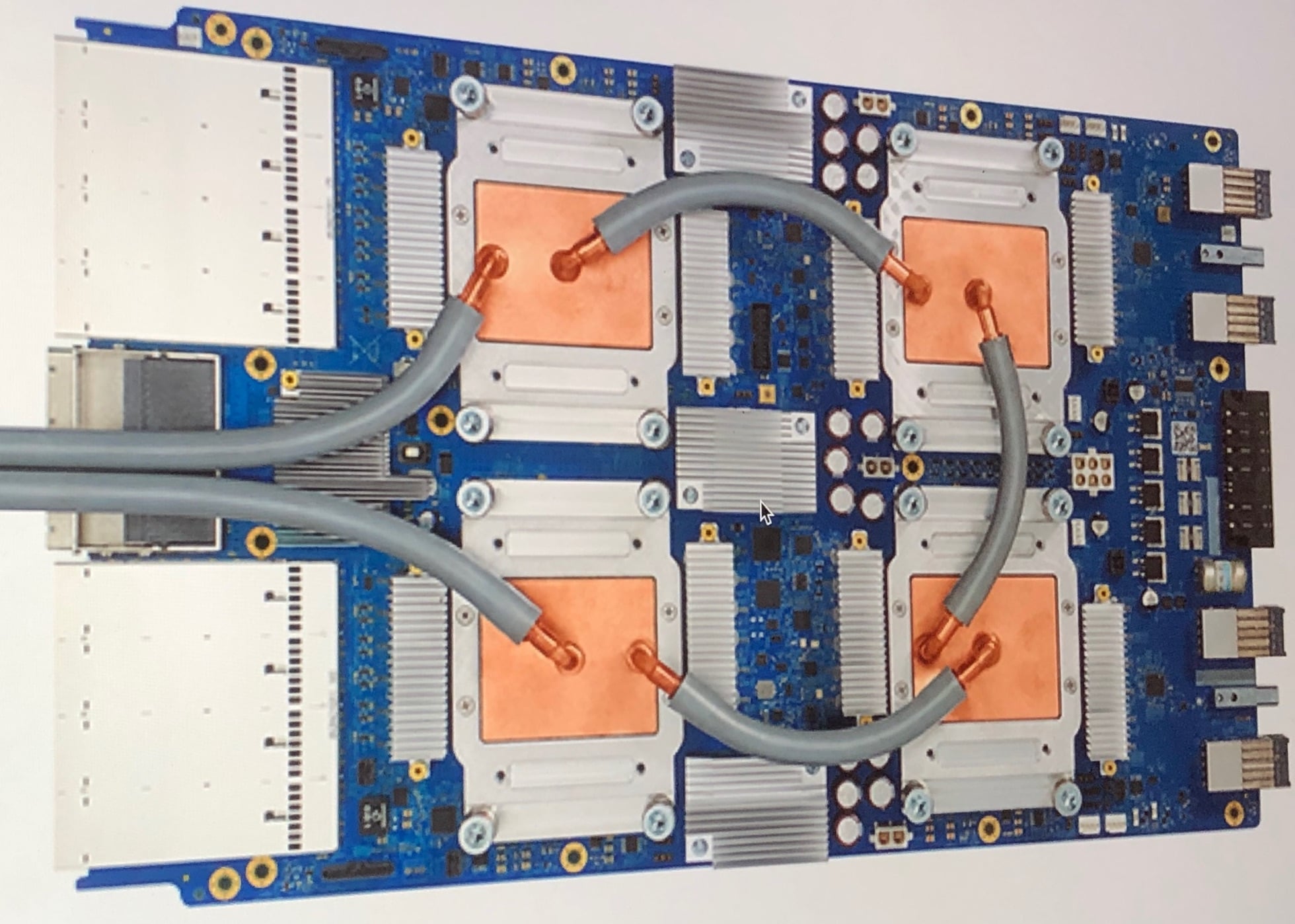
NVIDIA's first chip, NV1, had to deliver something close to a million-dollar Silicon Graphics workstation for a few hundred dollars. So the team optimized hard against the binding constraint of 1993, which was memory: DRAM cost roughly $50 per megabyte, and every byte you save is bandwidth you get back. Three choices followed, and all three were defensible:
Huang's summary: "We got it exactly wrong." And the lesson he draws is not about memory at all:
"Developers is everything. If you don't create an architecture and a computing platform that's easy for developers… it is simply not going to be adopted no matter how cost-effective it is."
The company was simultaneously under contract to build Sega's next-generation console on that architecture — a contract whose payments were the only thing keeping the lights on. Huang called Sega's chief executive, explained that NVIDIA was on the wrong path and would take Sega down it too, asked to be released from the contract, and then asked to keep the money anyway. Sega agreed. His rule for that kind of decision has outlived the crisis:
"Make the right decision first. The consequence you will think about second."
Then they built RIVA 128 in about nine months, by inverting how a schedule is normally written:
"Instead of saying this is the chip we have to build, how long is it going to take? We started with this is how much time we have — and how do we build such a thing?"
Read that beside Chang's story and the pairing is exact. Chang's lesson is that the process decides whether the product exists. Huang's is that the developer decides whether the process mattered. A perfectly manufactured chip nobody can program is scrap that passed final test.
🧾 What Did Morris Chang Actually Measure? (Not Yield)
Here is the twist in the story, and it comes from Chang's own mouth. He did not evaluate his factory managers on yield. Asked on stage in 2007 how he judged a fab manager, he described a dinner with the chief executive of a large integrated manufacturer who had just hinted at entering the foundry business. Chang asked him, innocently, how he evaluated his fab managers. The answer was a list of ten or twelve items, beginning with yield, cycle time and productivity. Then the man asked Chang the same question:
*"I said: no, no, no, John. I evaluate them according to how much complaint I get from customers about their fab. And that's the honest truth… We don't even keep P&L in each fab. But we do keep very good track of how satisfied the customers are. If a fab manager has got a very unsatisfied customer, he is in big trouble — I don't care how much money he makes."*
That is not a rejection of yield. It is a claim about where a metric belongs. Yield is what the process is tuned on. The customer's complaint is what the manager is judged on — because it is the only number that cannot be gamed from inside the building.
This matters directly for anyone measuring an AI system. Building a true yield instrument for generated software is hard — it needs a judge that can decide whether the output actually works, which is the unsolved verification problem. Chang's answer routes around it entirely: let the customer run the test, and instrument the complaint. In software that means republish loops on the same app, abandonment after first publish, error-fix invocations per project, share links that never get a second visit. None of those need a judge. All of them are already flowing through the product.
🧮 Why Did TSMC Refuse to Sell Customers a Share of the Fab?
Competitors in the 1990s offered joint ventures: co-invest in a fab, get a matching share of its capacity. It sounds fairer than queuing. Chang refused, and his reasoning was the growth rate of his best customers.
A reserved slice caps you at your own forecast — and the customer who matters is precisely the one whose forecast is wrong. NVIDIA grew roughly fivefold in a single year in that era. Huang did the arithmetic on stage himself, and it is the best one-line argument against capacity reservation anyone has made:
"If NVIDIA had invested in 20% and got only 20% of the fab's capacity — and in a few months you have outgrown the capacity you're supposed to get — then what would happen?"
Huang: "I would be a peaceful CEO running a $37 million company today."
   RESERVED SLICE vs SHARED POOL — the same fab, two contracts   Joint venture:   customer buys 20% of the fab  →  gets 20% of capacity
                    customer grows 5x in one year →  needs 100%
                    result: STRANDED at 20%, and the fab cannot help
   Shared pool:     customer buys nothing         →  gets what it needs
                    fab reinvests all profit into capacity
                    result: "we satisfied most of our customers, and we
                             PLEASED all of our important customers —
                             those that grew very fast"
   The lesson: when customer growth rates are widely dispersed, a shared
   flexible pool beats reserved slices FOR BOTH SIDES. The reservation
   protects you from the scenario you should be hoping for.
So the pure-play promise was never only about neutrality. It was also about non-allocation — refusing to pre-commit the factory, so the factory could follow demand instead of a contract.
🌍 Did Morris Chang Change His Mind About Free Trade?
Yes, and he is one of the few people who can be quoted on both sides of the argument. Asked at the Computer History Museum in 2007 whether America should worry about chip fabs moving offshore, he said no — with one narrow qualifier. Speaking at MIT in October 2023, at 92, he said the opposite.
| Question | Chang in 2007 | Chang in 2023 |
|---|---|---|
| Globalization | "It's a globalized world now" | "No globalization, no free trade, no free market" |
| Offshore commercial fabs | "I wouldn't worry too much" | Onshoring makes the industry "less efficient and less resilient" |
| Domestic capacity | Keep "enough… to satisfy our defense requirements" | National security "overrides everything" |
What did not change is the carve-out. In 2007 the defense exception was a single clause qualifying a confident free-trade position. By 2023 that exception had expanded until it governed the whole industry, and the free-trade position survived only as a lament about what the exception costs. Chang's principles held still; the scope of "defense-relevant" moved underneath him.
He is a hostile witness in both directions, which is what makes both quotes worth having. In 2007 he argued against protecting an industry he had every commercial reason to want protected. In 2023 he argued against the industrial policy funding his own company's Arizona fabs. And he left behind the one falsifiable claim in the whole debate — the mechanism is cost, not sovereignty:
*"The pervasiveness of chips is due to supply chain efficiency. If chip costs increase, its pervasiveness will lessen."*
👔 Who Actually Ran TSMC, and When?
Chang was chairman from the founding in 1987, not chief executive. Philips, an early investor, supplied TSMC's first CEO, James E. Dykes. Chang's own CEO tenure came later and in two separate stints, separated by four years.
| Period | Morris Chang's role |
|---|---|
| Feb 1987 → 1998 | Chairman (Philips supplied the first CEO, James E. Dykes) |
| Mar 1998 → Jun 2005 | Chairman and CEO |
| Jun 2005 → Jun 2009 | Chairman |
| Jun 2009 → 12 Nov 2013 | Chairman and CEO (second stint) |
| Nov 2013 → 5 Jun 2018 | Chairman; CEO duties to co-CEOs Mark Liu and C.C. Wei |
The "founder-CEO for eighteen straight years" version of this story is wrong in both directions: it gives him a title he did not hold in 1987 and merges two separate stints into one run. Chang retired on 5 June 2018, thirty-one years after incorporation.
📏 Do "3nm" and "2nm" Mean Anything Physical?
No. They are marketing names for process generations, not measurements. Nothing on a 3nm chip is 3nm across. Transistor pitch on an N3-class process is closer to 48nm — roughly 1,500 times finer than a human hair, which is impressive without needing to be exaggerated.
The features that genuinely measure a handful of nanometres are specific structures: nanosheet channel thicknesses and fin widths in the 5–10nm range, which really are thousands of times thinner than a hair. But the node number on the marketing sheet is a generation label, not a ruler reading, and has been for over a decade. Treat "3nm" the way you treat a car model year.
Being pedantic here matters for the same reason yield matters: the marketing number and the engineering number diverged, and the industry kept using both. The AI industry is currently repeating the pattern.
📊 Why Does the AI Industry Measure Capability but Almost Never Measure Yield?
Chang made yield the master metric of an entire industry — the one number the factory is organized around. The AI industry measures capability relentlessly, through benchmarks, leaderboards and evaluation suites, and measures yield almost never. But the yield numbers are everywhere once you know the unit to look for. Each of the results below was reported publicly by the team that produced it, and none of them were framed as yield:
| Publicly reported result | Yield reading |
|---|---|
| AlphaProof solved 9 of 353 Erdős problems | 2.5% good die per wafer |
| An engineering team's agent PR-success ramp, ~20–30% → ~80% | A textbook yield ramp on a production line |
| An overnight research loop producing 20 genuine improvements from 700 experiments | 2.9% — and the 680 failures still cost compute |
| An agentic review pipeline catching a mistake in 63% of ~1,000 changes across 59 repos | A defect-detection rate, measured like final test |
Every one of those is stated in Chang's units — good units out of units started — and almost none of them are reported that way. We unpack that unit in full in what yield means for AI systems. And the moment you accept the unit, the arithmetic that governs a fab starts governing agent runs too, because yields multiply along a chain:
   SERIAL YIELD:  Y = y₁ × y₂ × y₃ × … × yₙ   A 30-step agent run:
     99.0% per step  →  0.99³⁰  =  74%   "excellent benchmark, one in four runs fails"
     95.0% per step  →  0.95³⁰  =  21%   "good benchmark, four in five runs fail"
     90.0% per step  →  0.90³⁰  =   4%   "respectable benchmark, effectively unusable"
   The per-step number barely moved. The end-to-end number collapsed.
This is the quantitative reason long-horizon agent autonomy degrades in a way per-step benchmarks never show. A model that is 95% reliable on any individual action sounds close to solved. Chain thirty of those actions and four runs in five contain at least one error. Our writeup on how AI agents actually stay reliable covers the complementary half of the algebra — independent checkers, where miss rates multiply in your favour instead of against you.
Chang's doctrine points at the fix, and it is not more inspection. A fab buys yield by raising each individual step and encoding quality into the process — in software terms, agent evaluations at the step level, guardrails that fire before a bad state propagates, deterministic gates rather than a vibe check at the end, and a harness that can retry one step instead of a whole run. It is also why AI-generated apps break the way they do: the failure was manufactured thirty steps ago and only observed at final test.
One more Chang lesson is buried in that table. Final test must be independent of the thing being tested. A wafer probe is a separate machine with its own calibration. When the model that wrote the code also certifies the code, you have a probe wired to the stepper — a failure mode production agent deployments hit constantly.
🧬 What Does the Foundry Trade Look Like in Software?
The foundry trade is a clean division of labour: the customer brings domain intent, and the factory brings manufacture. Taskade Genesis makes structurally the same trade — you describe the app you need in a prompt, and the platform assembles the working version, with the projects, agents and automations wired up behind it.
That trade is why a foundry matters. A chip designer in 1990 could ship a product without ever touching a stepper. A clinic owner or a field-services operator in 2026 can ship a working internal tool without ever touching a deployment pipeline. In both cases, somebody with deep domain knowledge and no manufacturing capability got access to a factory.
| The foundry trade | Taskade Genesis equivalent |
|---|---|
| Customer supplies the design intent | You supply the prompt and the domain knowledge |
| Foundry supplies the process node | The platform supplies generation, hosting, custom domains and SSL |
| Customer never touches a stepper | You never touch a build pipeline — see your first app |
| Test and binning before shipment | Version history and error fixing before you publish |
| Packaged parts ship to market | Publishing an app to your own domain or the Community Gallery |
One honest caveat, because the analogy has a limit. TSMC's founding promise was neutrality — we will never compete with our customers. Taskade does not make that promise and should not pretend to. Taskade ships first-party starter kits, and published apps are surfaced in the Community Gallery where other people can clone them. The accurate description is a foundry with a starter library, not a pure-play foundry. That may well be the better business — the next builder skips the blank prompt entirely — but it is a different arrangement from the one Chang made in 1987.
The yield idea transfers exactly, though. On the execution side, Taskade already reports something Chang would recognize: automations carry a health signal computed from recent run history, and every run keeps a step-by-step log with per-step inputs and outputs. That is process control, not a satisfaction survey — it tells you which step is dragging the line down. Extending that discipline from automations to everything an AI agent manufactures is where the whole industry is heading, whether it calls the number "yield" or not.
Memory feeds Intelligence, Intelligence triggers Execution, Execution creates Memory — the Workspace DNA loop is a production line, and production lines have yields. Build your first app free →
🕰️ Morris Chang and TSMC: The Timeline
Morris Chang's career spans sixty years, from a near-zero yield line at Texas Instruments in 1958 to a $2.16 trillion company he retired from in June 2018. The dates below are the load-bearing ones, and several of them contradict the version of this story that circulates online.
| Year | Event |
|---|---|
| 1931 | Born 10 July in Ningbo, Zhejiang |
| 1937–1943 | Guangzhou → Hong Kong → occupied Shanghai → 50-day crossing to Chongqing |
| 1949 | Flies Pan Am from Kai Tak to San Francisco; Harvard freshman year |
| 1952–1953 | MIT — BS then MS in mechanical engineering |
| ~1955 | Fails the MIT doctoral qualifier twice; chooses Sylvania over Ford by one dollar |
| 1958 | Joins Texas Instruments; assigned the yield problem — and runs a line doing foundry work for IBM |
| 1964 | PhD in electrical engineering, Stanford — funded by TI |
| 1976 | Pitches a foundry model inside TI; rejected |
| 1981 | Miho fab in Japan runs 40–50% memory yield, roughly double Houston's |
| ~1983 | Leaves TI at 51 after 25 years; president and COO at General Instrument |
| 1985 | Recruited by K.T. Li to head ITRI in Taiwan |
| 1987 | TSMC incorporated 21 February; Andy Grove visits in late 1987; Intel becomes first American customer |
| 1993 | Jensen Huang calls TSMC's local sales office; nobody calls back (his own account, 2007) |
| 1997–1998 | Huang's letter reaches Chang; deal signed 1998; RIVA TNT is the first fully-TSMC NVIDIA part |
| 2007 | Huang interviews Chang at the Computer History Museum — the customer-complaint metric, the JV refusal |
| 2023 | Chang at MIT, aged 92: "No globalization, no free trade, no free market" for chips |
| 1998–2005 | Chairman and CEO |
| 2009–2013 | Chairman and CEO, second stint |
| 2018 | Retires as chairman on 5 June |
| 2026 | ~$2.16 trillion market cap; 6th most valuable company in the world (23 July) |
🤔 What Is the Lesson of Morris Chang's Career?
The lesson is that an interface can be worth more than an invention. Chang did not invent the transistor, the wafer, or lithography. He drew a line between two activities that had always been done by the same company, and let a different firm stand on each side of it.
That is a repeatable move, and it keeps happening. Hosting accounts separated running a website from owning a server. Cloud computing separated running software from owning a data center. Open-weight models separated owning a model's design from being able to manufacture its inference — publishing the blueprint changes who owns it and nothing about who can run it.
It comes with a warning too: the layer that creates the value does not automatically capture it. Telecom carriers moved orders of magnitude more data over twenty-five years and their equities went nowhere. TSMC captured the profits of its split. Most infrastructure does not. "We are the foundry of X" has to be earned in margin, not asserted in a keynote.
The second lesson is quieter and more useful. Chang won by caring about a number nobody else found interesting. Everybody in 1958 wanted to talk about what a transistor could do. He spent forty years on what fraction of them worked. The capability question is the fun one, and the industry is full of people asking it. The yield question is the one that decides whether a factory — of chips, of software, of agent runs — is a business or a demonstration.
🐑 Before you go... Taskade turns the same trade into a workspace: you bring the domain intent, the platform manufactures the working system.
🤖 AI Agents: persistent memory, a large built-in toolset, and 100+ bidirectional integrations — triggers pull events in, actions push data out.
⚙️ Automations: workflows with a per-run log and a health signal computed from recent runs — process control, not guesswork.
🧬 Taskade Genesis: one prompt, one deployed app. Explore what other people have built, or start from ready-made AI apps.
Memory ▲ · Intelligence ■ · Execution ● — the loop Chang would have called a line, with a yield you can actually read. Start building free 👈
🔗 Resources
Computer History Museum oral history — Morris Chang interviewed by Alan Patterson, 24 August 2007 (CHM ref X4151.2008)
張忠謀,《張忠謀自傳》(Morris Chang autobiography), Vol. 1 1998 / Vol. 2 November 2024, 天下文化
Brian Potter, Construction Physics — on the founding of TSMC and the pure-play model
Chris Miller, Chip War: The Fight for the World's Most Critical Technology
💬 Frequently Asked Questions About TSMC and Morris Chang
What does TSMC stand for?
TSMC stands for Taiwan Semiconductor Manufacturing Company. It was incorporated on 21 February 1987 and is headquartered in Hsinchu, Taiwan. It is the world's first and largest pure-play semiconductor foundry.
Why doesn't TSMC design its own chips?
Because designing its own chips would break the promise the company was built on. A fabless customer hands a foundry its most valuable intellectual property. If the foundry also sold competing products, that hand-off would be arming a rival. Neutrality is the product, and it is why thousands of chip companies exist that could never have afforded a factory.
How big is TSMC compared to other semiconductor companies?
As of 23 July 2026, TSMC's market capitalization is roughly $2.16 trillion, making it the sixth most valuable company in the world. It crossed $2 trillion on 25 February 2026. By most estimates it manufactures around 90% of the world's leading-edge logic chips at 5nm and below and about 70% of the total foundry market including mature process nodes.
What is the difference between a foundry and a fabless company?
A fabless company designs chips and owns no factory. A foundry owns the factory and manufactures other people's designs. NVIDIA, Qualcomm, AMD and Apple's silicon group are fabless. TSMC is a foundry. The split only became viable once a foundry existed that would never compete with the designers it served — which is the split TSMC created in 1987.
Who was Morris Chang before he founded TSMC?
Morris Chang was born on 10 July 1931 in Ningbo, Zhejiang. He fled war three times as a child, lived in six cities and changed schools ten times before turning eighteen. He spent one year at Harvard, transferred to MIT for mechanical engineering, failed the MIT doctoral qualifying exam twice, and joined Texas Instruments in 1958 — where he was handed the yield problem. He earned a PhD from Stanford in 1964 and founded TSMC in 1987, at 55.
Did TSMC manufacture the NVIDIA RIVA 128?
Partly — and both the flat "yes" and the flat "no" are wrong. The original RIVA 128 (NV3) launched on 25 August 1997 built by SGS-Thomson on 350nm, which had been NVIDIA's fab partner since NV1. NVIDIA then moved the RIVA 128 ZX variant to TSMC after yield problems and pressure from its investors, so the NV3 generation was manufactured by both companies. The first fully-TSMC NVIDIA part was the RIVA TNT, launched on 31 August 1998. The reason for the switch is the theme of this whole article: the dies were not coming out.
Do "3nm" and "2nm" describe a physical measurement?
No. They are marketing names for process generations, not dimensions. Nothing on a 3nm chip measures 3nm. Transistor pitch on an N3-class process is closer to 48nm, roughly 1,500 times finer than a human hair. The structures that genuinely are a few nanometres across are specific features such as nanosheet channels and fin widths — not the number printed on the node name.
How is serial yield relevant to AI agents?
Yields multiply along a chain. A 30-step agent run at 99% reliability per step succeeds 74% of the time; at 95% per step it succeeds 21% of the time. Per-step benchmarks look strong in both cases, which is why long-horizon reliability collapses invisibly. The fix is the one a fab uses: raise each individual step and put an independent check between steps, rather than inspecting only at the end.
How does Taskade Genesis relate to the foundry model?
Taskade Genesis performs the same division of labour — you bring the domain intent, the platform manufactures the working app, and you never touch a build pipeline. The honest difference is neutrality: TSMC promised never to compete with its customers, while Taskade ships first-party starter kits alongside customer-built apps. The accurate label is a foundry with a starter library.
What does Taskade cost?
Taskade has a free plan. Paid plans start at Pro, $10/month billed annually, then Business at $25/month billed annually, Max at $100/month, and Enterprise at $250/month, all billed annually. Every paid tier includes AI agents, automations, and Taskade Genesis app building with 15+ frontier models from OpenAI, Anthropic, Google, and open-weight providers.
🧬 Build Something That Ships
TSMC made it possible to sell a chip without owning a factory. Taskade Genesis makes it possible to ship an application without owning a build pipeline — one prompt, one app, with AI agents, automations, and 100+ integrations wired in. Browse what other people have built, or start from a working app.